Graphene, a single-atom thick sheet of carbon, has become the focus of a lot of research (and a Nobel Prize) because it has an interesting electronic property: electrons move through the material as if they have no mass. But it's only one of a number of single-atom thick materials that have been discovered, and some of the others have very different properties, acting as semiconductors or insulators.
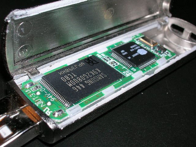
The discoveries raise the prospect of building more complex electronic devices out of a series of these materials, with each part being only a single atom thick. Now, researchers have used two of these materials—graphene and molybdenum disulfide—and put them together with some more traditional components to make a flash memory device. Although the work is very preliminary, with some of the parts being assembled by hand under a microscope, it shows some excellent properties, like the potential to store more than one bit per device and the ability to retain its state for over a decade.
The basic outline of a flash memory device involves two electrodes that feed current through a semiconductor within the device. When a negative voltage is sent across a device from a control electrode, electrons are able to feed into a reservoir that retains the charge; reversing the voltage allows them to escape. The presence of the electrons in the reservoir can be read out by sending current through the semiconductor.
To build a compact version of the device, the authors of the new paper (who are based in Lausanne, Switzerland) started with two sheets of graphene layered on some silicon, separated by a small gap. These served as the electrodes, with the device itself acting as a bridge between them. The next layer on top of that was the semiconductor, formed by a single-molecule-thick sheet of molybdenum disulfide. Above that, a layer of an insulator that allows electrons to tunnel through it separated the conductor from the charge reservoir. To hold the charges, the authors used a few layers of graphene. That was topped by a bit more insulator and another electrode that acted to control the device, setting it to read or erase.
The insulator used in this work wasn't a single atom thick (although insulators of this sort are known) and the graphene charge reservoir was several layers thick, so there were clearly a number of layers involved. Still, this is a very thin device, and it can potentially be made even thinner. The manufacturing technique could use some improvements as well, given that one of the steps involved finding individual layers using an optical microscope.
In any case, the devices worked. Applying a positive voltage to the control electrode allowed charge to accumulate in the graphene layers, and its presence could be read out based on the current flowing through the device. Reversing the voltage across the control electrode erased the device. They went through 120 write/erase cycles, and the device still functioned. They also left the device unpowered for a while and found that while its storage did decay a bit, it only decayed very slowly. Based on the rate, they expect that 30 percent of the original charge would still be present after 10 years.
The difference in current between the clear and charged state was also very large, with the ratio between the current flowing in them being 104. That should allow a single device to encode a number of distinct states, meaning it can store multiple bits, a technique already in use in multilevel flash memory.
Like graphene, molybdenum disulfide is flexible, meaning that it could potentially find uses in some non-traditional electronics. And the authors seem confident that devices based on it can be mass-produced with techniques that are already established. Still, it's clear that there are a number of issues to be worked out before this is ready for the factory floor.
ACS Nano, 2013. DOI: 10.1021/nn3059136 (About DOIs).
reader comments
31