New silicon-containing circuits dissolve when wet. Dissolvable electronic devices might be useful for smart medical implants or environmental sensors, their developers say.
Silicon is a relatively inert material, which makes it useful for electronic circuits in computer chips and solar cells. But that same characteristic becomes problematic if you want to build an implantable biosensor, for example. Silicon-based circuits in the device will stay in the body indefinitely.
Scientists have built partially biodegradable transistors using organic semiconducting polymers or molecules. But organic semiconductors don’t carry charge as well as their silicon counterparts. While it’s possible to build individual transistors, diodes, and memory in the lab using organic semiconductors, combining these circuits into a microprocessor is harder than working with silicon parts, says Zhenan Bao at Stanford University, who was not involved with this current study. That’s because silicon-containing circuits have a longer history of development due to their widespread use in the semiconductor and electronics industries.
As a result, building an electric circuit for biodegradability and performance required some compromises—until now. John Rogers, at the University of Illinois, Urbana-Champaign; Fiorenzo Omenetto, at Tufts University; and their colleagues have built water-soluble, silicon-containing circuits.
In traditional silicon circuits, charges flow along the top layers of the material. So by building a circuit with a thin semiconducting layer, the researchers hoped to retain the device performance while improving its solubility in the slightly alkaline conditions of our blood.
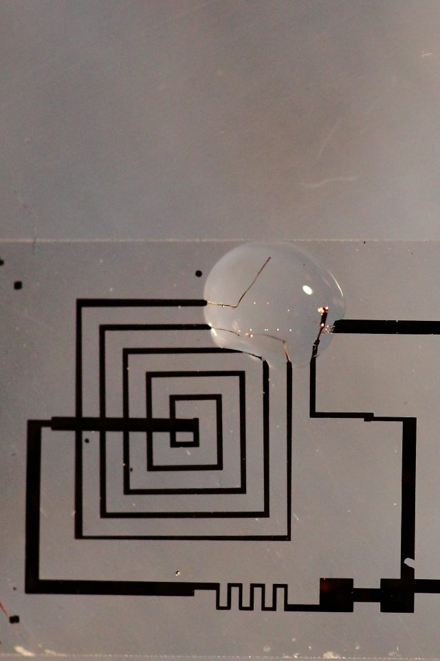
The researchers sliced sheets of silicon, up to 300 nanometers thin, from a wafer and stamped those sheets onto silk. Then they patterned magnesium electrodes and magnesium oxide (or silicon dioxide) dielectrics around the silicon semiconductor. Finally, the scientists wrapped the circuit in a synthetic cocoon of silk protein. The composition of the silk covering determines how quickly the wrapper, and thus the device, dissolves.
The scientists used these materials to build a large collection of devices: diode, transistor, capacitor, logic gate, solar cell, strain sensor, temperature sensor and LC oscillator. They also combined dissolvable diodes to make a 64-pixel photodetector for a digital camera, which could possibly be powered by a dissolvable solar cell.
In one more demonstration, they built a biodegradable medical device with their new circuit design. The researchers implanted a silk package containing magnesium inductive coils and silicon microheaters at surgical site in a mouse. (Silicon and magnesium are biocompatible. Porous silicon nanospheres might be useful containers for drug delivery and stents containing magnesium hold open blocked arteries.)
Wireless signals activated the device, which warmed the tissue about 5°Celsius and killed bacteria in the wound. The device dissolved after 15 days, leaving some longer-lasting silk fibers behind.
The experiment simulates an antibiotic-free way to prevent infections at an incision immediately after surgery, Rogers says. He also envisions using these dissolvable circuits to build environmental sensors that disappear without a trace or even incorporating them into consumer electronics to reduce electronic waste.
For dissolvable electronic circuits to become widespread, though, engineers need to figure out how to manufacture them using current semiconductor industry fabrication techniques, Rogers says. He’s working on that problem and is optimistic that it’s can be solved.
Science, 2012. DOI: 10.1126/science.1226325 (About DOIs).
reader comments
16