Graphene—a two-dimensional sheet of carbon one atom thick—is exciting stuff. Combining good electrical properties, flexibility, mechanical strength, and other advantages, graphene can seem like a miracle material, especially when potential applications are listed. Talk of graphene-based protective coatings, flexible transparent electronics, super powerful capacitors, and so forth may seem like something from a Neal Stephenson science fiction novel, but they've all been seriously considered.
The material's potential is so high that its discovery merited the 2010 Nobel Prize in physics, awarded to Andre Geim and Konstantin Novoselov. Certainly my fellow Ars Technica writers and I have spilled a lot of digital ink on the subject.
However, with so much excitement, you would be forgiven for wondering if at least some of it is hype. (After all, graphene has been around for a number of years, but we don't have our transparent computers yet.) For this reason, Nobel Laureate Konstantin Novoselov and colleagues have written a critical, yet optimistic, assessment of the state of graphene research and production.
As they point out, there is a big question that must be answered before widespread adoption of graphene technology is possible: are graphene's advantages sufficient to use it in place of the materials we use in existing devices? The authors conclude that, to some extent, that's the wrong question. Graphene's biggest promise lies in novel applications, designed especially for the advantages that graphene offers.
What's the big deal about graphene?
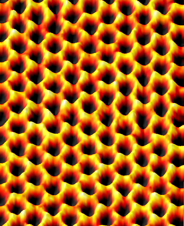
Graphene was the first material discovered that consists of a single layer of atoms. (Other single-layer materials, including boron nitride and molybdenum disulphide, were subsequently discovered. In fact, graphene and boron nitride together have proven to be an effective composite material.) As shown in the scanning microscope image above, graphene forms a hexagonal lattice of carbon atoms. Multiple layers of graphene form the familiar substance graphite, used in pencils and as a mechanical lubricant; carbon nanotubes are graphene sheets rolled into a cylinder.
Due to the nature of the bonds between the carbon atoms, graphene is very resilient: the sheets can be bent at severe angles before fracturing and withstand high pressure. Since the material consists of only one layer of atoms, electron motion is confined to a single plane, which gives rise to novel electrical properties. Graphene is also transparent at optical wavelengths, and impervious to gas. Together, these properties make graphene desirable in protective films, as well as transparent, flexible electronic devices.
Production methods, costs, and quality
The amazing research we've seen being performed with graphene has all relied upon high-quality samples. As you might expect, achieving the best electrical and mechanical properties requires the most expensive and painstaking process: mechanical exofoliation. In this technique, graphene flakes are individually extracted using adhesive tape. This process is not scalable, so it is essentially useless in manufacturing terms.
Other methods are far more scalable, but currently trade off on quality.
- Liquid-phase exfoliation involves suspending carbon-carrying materials (such as graphite) in a liquid with high surface tension, then bombarding the suspension with sound to extract graphene flakes.
- Chemical vapor deposition (CVD) condenses a volatile substance containing carbon onto a copper surface. The graphene layer that forms can then be peeled off onto another substrate. CVD is frequently used to make other thin-film systems for electronic devices.
- Growing graphene directly onto a silicon carbide wafer by selectively extracting the silicon atoms in the top layer via sublimation (vaporizing a solid).
This list isn't exhaustive, but it shows that many methods are available. While none of them currently produce as high quality graphene as mechanical exfoliation, CVD in particular is a promising method, and much less expensive.
Not all of these methods are equally useful for all applications, though. Some are best for making protective coatings, while others (which I've focused on here) are better for electronics, particularly nanoelectronics.
Where's my bendy laptop?
Beyond fabrication costs and quality, graphene-based electronics must overcome certain obstacles to be practical. Touch screens, electronic "paper", and other display-based media require improvements in the electrical resistance at the junction between the graphene and metal electrodes. The authors of the review wrote that they expect this problem will be solved in the next decade.
So why can't we make the whole device from graphene? While some progress has been made on graphene transistors, they aren't production-ready yet. Semiconductor transistors, which are the foundation of modern electronics, have a particular electronic property known as a bandgap: a transition point that allows an asymmetric flow of charge through circuits. Pure graphene lacks a bandgap; research is ongoing to address the problem (by using multiple layers, adding other elements, and/or making structural changes), but Novoselov et al. speculated graphene integrated circuits are at least a decade off.
As a result, graphene is not poised to replace conventional semiconductor components any time soon. However, in areas where no conventional devices exist—flexible and transparent electronics—graphene-based electronics could arrive in consumers' hands in the next decade or so. Maybe it won't be a bendable cell phone you can put in the back pocket of your jeans, but it's a safe bet that graphene will be moving from the laboratory into the wider world relatively soon.
Nature, 2012. DOI: 10.1038/nature11458 (About DOIs).
reader comments
33